

PCBs are at the core of electronic products. Traditional manufacturing and 3D printing each have their own characteristics. How should one choose?
Process Principles
Traditional PCB manufacturing is a subtractive process. Dongguan Jingwei Communication Technology's services begin with PCB design, followed by optimisation through PCB layout services, and then completed through processes such as photolithography and etching. The process is mature and stable.
3D printing is an additive manufacturing process that does not require traditional PCB layout services for planar wiring. Based on PCB design logic, it uses 3D modelling software to design the circuit, then prints conductive and insulating materials layer by layer to form a three-dimensional circuit, enabling rapid design realisation.
Material Characteristics
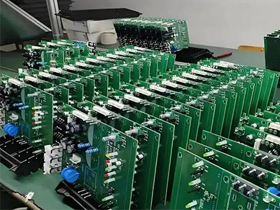
PCB manufacturing materials are fixed and related to PCB solution design. Substrates are primarily FR-4, with copper foil used for conductors, meeting the signal requirements of PCB design.
3D printing offers diverse materials, providing innovative possibilities for PCB solution design, including polymers and flexible materials. However, some conductive materials have inferior performance compared to copper foil, limiting their application in high-demand PCB designs.
Precision and Structure
Traditional processes achieve high precision, with line width/spacing as fine as 3 mil/3 mil, suitable for intricate PCB designs. PCB layout services play a significant role, but they struggle to produce complex three-dimensional structures.
3D printing offers high three-dimensional freedom, helping PCB solution design break through limitations and enabling the production of special structures. However, precision is slightly lower at 100-200μm, making it difficult to meet high-demand PCB design requirements.
Cost and Application
Traditional manufacturing offers cost advantages for large-scale production. Standardised PCB design and PCB layout services enhance efficiency, making them suitable for high-volume fields such as consumer electronics.
3D printing is cost-effective for small-scale production and prototyping, suitable for rapid validation of PCB design, and ideal for customised products. When combined with PCB solution design, it can achieve unique functionalities.
In summary, the choice should be based on factors such as precision and scale. For large-scale, high-precision applications, traditional manufacturing with PCB design and layout services is recommended; for small-scale, customised applications, 3D printing with innovative solution design is preferred.