

In the PCB manufacturing industry, scrap rates are a key indicator of production efficiency and cost control. Dongguan Jingwei Communication Technology Co., Ltd. has been deeply involved in the PCB industry. By integrating DFM principles throughout the entire PCB design process, the company has successfully helped clients reduce PCB scrap rates by over 30%, providing reliable support for the mass production of high-precision products such as Energy Storage Board PCBA and Inverter PCBA.
The core of DFM lies in fully considering production feasibility during the design phase to avoid scrap caused by the disconnect between design and manufacturing. In traditional PCB layout services, designers often prioritize functional density over production process constraints, such as overly narrow trace widths or too-small pad spacings, which can lead to uneven etching or soldering short circuits, directly resulting in batch scrap. Jingwei Communication's PCB Solution Design team involves manufacturing engineers in the review process from the early stages of design. Based on production line parameters such as laser drilling precision and solder mask printing tolerances, they optimize design elements like trace width, spacing, and hole size to minimize design risks that are difficult to achieve in manufacturing from the outset.
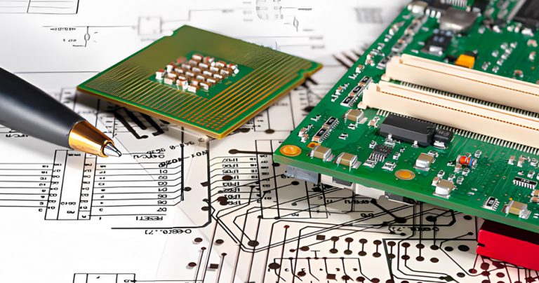
For products like Energy Storage Board PCBA that have extremely high thermal dissipation requirements, DFM optimization is even more targeted. The design team simulates soldering temperature curves to adjust copper foil thickness and layout, avoiding solder joint defects caused by localized poor thermal dissipation. They also match component layout with the nozzle size of the pick-and-place equipment to reduce scrap caused by placement misalignment. In the high-voltage area design of Inverter PCBA, DFM focuses on controlling creepage distance and insulation layer thickness, combined with AOI inspection capabilities during production, to ensure design parameters fall within inspection accuracy ranges, thereby reducing scrap caused by failed voltage withstand tests.
DFM can also enhance production compatibility through standardized design. Jingwei Communications has established a database in PCB design that includes common component packages and routing rules, enabling the reuse of design outcomes across different projects and reducing equipment debugging time and material waste caused by design differences. For example, standardizing solder mask window sizes reduces stencil replacement frequency and avoids batch scrap caused by alignment deviations; standardized via diameters improve plating uniformity and reduce defects such as via wall voids.
From PCB layout services to mass production delivery, the integration of DFM creates a closed-loop system between design and manufacturing. Jingwei Communication uses DFM analysis software to link with production data and continuously iterate design rules. When a certain type of design repeatedly results in scrap during production, the system automatically flags it and suggests optimization directions, achieving a positive feedback loop of “design - manufacturing - feedback - optimization.” This approach of embedding manufacturability into the design DNA not only reduces PCB scrap rates but also shortens the time-to-market from design to mass production, creating significant cost advantages for customers.
In the precision manufacturing sector, DFM has become a core tool for cost reduction and efficiency improvement in the PCB industry. Dongguan Jingwei Communication Technology Co., Ltd. uses PCB Solution Design as a bridge to deeply integrate DFM into the entire PCB manufacturing process, leveraging design optimization to address production challenges and providing robust technical support for the efficient mass production of various PCB products.