

With the increasing popularity of high frequency electronic equipment, electromagnetic compatibility ( EMC ) has become the core index of product design. Based on years of experience in the field of PCB assembly ( PCB assembly ) and SMT manufacturing ( surface mount technology manufacturing ), Dongguan Jingxie Communication Technology Co., Ltd.summarized the key methods of EMC optimization in high-frequency PCB layout, providing practical reference for engineers.
In the high frequency circuit, the signal transmission speed can reach more than 1GHz, and the unreasonable layout is easy to cause electromagnetic interference ( EMI ) and electromagnetic sensitivity ( EMS ) problems. Firstly, it is necessary to pay attention to the grounding design, and adopt the combination scheme of ' star grounding + grounding plane ' : laying a complete grounding copper sheet on the top and bottom layers of PCB, and connecting the digital ground and the analog ground through a single point of 0 ohm resistance or magnetic beads to avoid the formation of ground loop. In the process of PCBA assembly, the impedance consistency of grounding solder joints will be strictly controlled to ensure that the grounding resistance is less than or equal to 5mΩ.
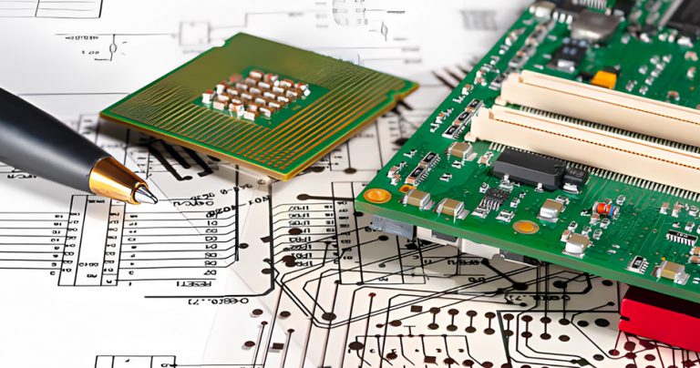
Signal routing is the key to EMC optimization. The high frequency signal line needs to adopt short straight wiring to avoid right angle turning. The turning point should adopt 45 degree angle or arc transition to reduce the impedance mutation. The differential signal line needs to maintain equal length and equal distance, the impedance matching is controlled within ± 10 %, and the matching resistance position is reserved at the end. The power supply wiring should adopt a thick wire diameter to reduce the line resistance. At the same time, 104 ceramic capacitors are placed near the chip power pin to achieve high frequency filtering. The SMT production line is equipped with a high-precision placement machine, which can ensure the wiring accuracy of 0402 and below packaging components and meet the needs of high-frequency signal transmission.
The layout of the components should follow the principle of ' functional partition ' : the high frequency oscillator, power amplifier and other strong interference sources should be far away from the sensitive circuit ( such as ADC, sensor module ), and the distance between the two is recommended to be ≥ 20 mm. For the RF module, the shielding area needs to be divided separately, and the metal shielding cover is used to isolate the shielding cover. The shielding cover is connected to the ground plane in multiple points to reduce the radiation leakage. In the turnkey PCBA assembly service, engineers will plan the layout partition in advance according to the schematic diagram to reduce the cost of later rectification.
In addition, PCB stack design also needs to be considered. The high frequency plate is recommended to use at least 4 layers of plate design, the signal layer and the ground layer are arranged alternately, and the ground plane is used as the shielding layer to reduce the interlayer interference. In the selection of plate, the substrate with low dielectric constant ( εr ≤ 3.5 ) should be selected for high frequency circuit to reduce the signal transmission loss. In the PCB assembly stage, the impedance test instrument will be used to test the impedance of the key signal line to ensure that the design requirements are met.
Dongguan JingLian Communication Technology Co., Ltd.has accumulated rich experience in the field of high frequency PCB, from PCB design audit, component selection to SMT placement and assembly test, providing full process turnkey service. The company is equipped with EMC test equipment, which can test the finished products such as radiation harassment and conduction harassment, and help customers quickly pass CE, FCC and other certifications. In the future, Jingli Communication will continue to optimize the high-frequency PCB manufacturing process and provide more reliable PCBA solutions for communication, medical, Internet of Things and other fields.