

The Imperative of PCB Layout Optimization in Compact Designs
From slim smart thermostats to portable medical monitors and miniaturized kitchen gadgets, the demand for compact appliances is reshaping consumer electronics. At the core of these space-efficient devices lies a well-optimized Printed Circuit Board (PCB) layout—where every millimeter counts. A poor layout can lead to signal interference, overheating, or compromised functionality, while a strategic design maximizes space, enhances performance, and ensures reliability. For PCB manufacturers, mastering layout optimization is the key to meeting the demands of today’s compact appliance market.
Core Strategies for Compact Appliance PCB Layout
Component Selection: Small Form Factors First
Optimization starts with component choices. We prioritize miniaturized parts such as 0201-sized resistors, BGA (Ball Grid Array) chips, and chip-scale packages (CSP) over traditional through-hole components. For example, replacing a standard DIP switch with a surface-mount equivalent reduces footprint by up to 60%. We also partner with trusted suppliers to source high-density components that maintain performance—critical for power-hungry compact devices like portable chargers.
Circuit Routing: Efficiency in Every Trace
Smart routing is non-negotiable for compact PCBs. We use autorouting tools paired with manual refinement to minimize trace lengths, reducing signal delay and interference. For high-frequency circuits (e.g., in smart home sensors), we implement differential pairing to cancel out noise. Additionally, we place power and ground planes strategically to create a low-impedance path, preventing voltage drops that can disrupt sensitive components in tight spaces.
Thermal Management: Prevent Overheating in Confined Spaces
Compact appliances trap heat, making thermal design a priority. Our layout teams position heat-generating components (e.g., voltage regulators) away from temperature-sensitive parts like microcontrollers. We also integrate thermal vias to dissipate heat to the PCB’s inner layers and use copper pours to spread heat evenly. For devices like mini air purifiers, this approach reduces operating temperatures by 15–20°C, extending component lifespan.
DFM Compliance: Manufacturability Meets Miniaturization
A great layout must be manufacturable. We adhere to Design for Manufacturability (DFM) rules, ensuring adequate spacing between components (minimum 0.1mm for SMT parts) and clearances for solder masks. This avoids issues like tombstoning during assembly and simplifies inspection. We also use HDI (High-Density Interconnect) technology for multi-layer PCBs, allowing us to stack circuits vertically without sacrificing space.
Case: Layout Optimization for a Mini Smart Thermostat
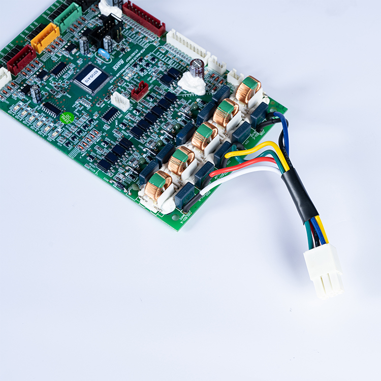
A client approached us to redesign the PCB for their 40mm×40mm smart thermostat, which suffered from signal interference and overheating. Our team replaced through-hole connectors with board-to-board pin headers, shrinking the component footprint by 30%. We then rerouted the Wi-Fi module’s traces to reduce crosstalk and added thermal vias near the power chip. The result? A 25% smaller PCB, 40% less signal noise, and a 12°C drop in operating temperature—all while maintaining the thermostat’s full functionality.
Our PCB Layout Optimization Services
As a specialized PCB manufacturer, we combine design expertise with advanced tools to deliver optimized layouts for compact appliances. Our team includes DFM engineers and thermal specialists who collaborate with clients from concept to production. We use 3D modeling software to simulate layout performance and offer rapid prototyping to test designs before mass production. Whether you’re building a wearable device or a mini home appliance, we tailor layouts to your space constraints and performance goals.