

As wearable devices quickly iterate towards "slim and small", the demand for miniaturization of their core components PCBs (printed circuit boards) is becoming increasingly urgent. As a professional PCBA assembly (printed circuit board assembly) service provider, Dongguan Jingqiu Communication Technology Co., Ltd. has been deeply engaged in turnkey pcba assembly (one-stop PCBA assembly), PCB assembly (PCB assembly) and SMT manufacturing (surface mounting technology manufacturing) fields for many years. In response to the challenges of material adaptation and process accuracy faced by wearable device PCB miniaturization, it has achieved breakthroughs through technological innovation to provide wearable device manufacturers with high reliability miniaturization PCB solutions.
The primary challenge in miniaturization of wearable devices PCBs is material selection. Traditional PCB substrates are prone to insufficient heat dissipation and insufficient mechanical strength in miniaturization scenarios. — Jingqiu Communications selected high-density interconnection (HDI) substrates, with a lower dielectric constant (controlled between 3.0 and 3.5), which can reduce signal transmission losses and adapt to the signal requirements of medium and high-frequency sensors of wearable devices; at the same time, ultra-thin copper foil (thickness as low as 12μm) is used to reduce the area of the PCB while improving the current carrying capacity to avoid heating problems caused by excessive lines. In addition, in view of the characteristics of wearable devices being close to the human body and needing frequent bending, Jingqiu Communications has introduced soft and hard bonding boards that combine flexible substrates and rigid substrates, taking into account miniaturization and durability, and the bending life can reach more than 100,000 times, meeting the use scenarios of smart bracelets, heart rate monitors and other products.
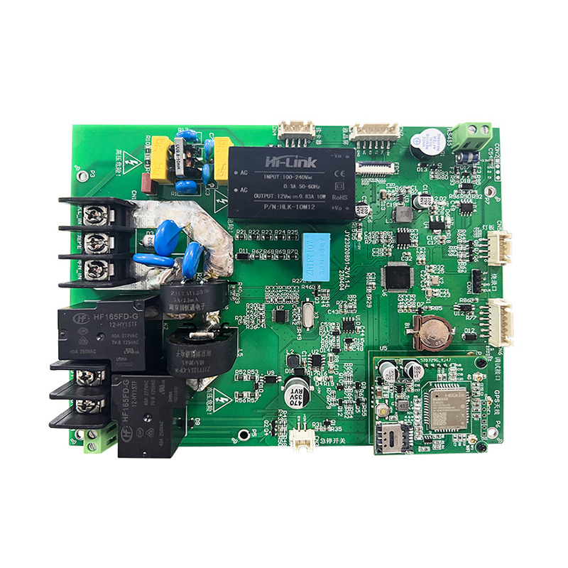
Process accuracy is the core bottleneck in the mass production of miniaturized PCBs. The line width and line spacing of wearable device PCBs often need to be controlled below 0.1mm, and it needs to be equipped with a large number of micro components (such as 01005 packaged chips), which puts high requirements on the SMT manufacturing process. Jingqian Communication has introduced a high-precision chip machine (positioning accuracy ±0.02mm), combined with 3D SPI (solder paste detection) equipment, real-time monitoring of solder paste thickness and printing quality, and increasing the component mounting yield to more than 99.8%. In the PCB assembly link, laser drilling technology (the minimum aperture can reach 0.1mm) is used to realize high-density line interconnection, and at the same time, through the vacuum reflow soldering process, the welding temperature curve is accurately controlled to avoid damage to micro chips due to high temperature. Taking a smart watch PCB as an example, through process optimization, Jingqiu Communication reduced the PCB area by 25%, while achieving stable assembly of 120+ components to meet the needs of lightweight equipment.
One-stop service capabilities solve the supporting problems of miniaturized PCBs for wearable device manufacturers. The turnkey pcba assembly service provided by Jingqiu Communication covers the entire process from PCB design optimization, component procurement to PCBA assembly, and finished product testing: During the design stage, engineers will optimize the line layout and heat dissipation path in advance according to miniaturization needs; in the component procurement process, relying on global supply chain resources to ensure the stable supply of micro components; in the finished product testing stage, customized testing fixtures are used to simulate the actual use environment of wearable devices, and comprehensively test the signal integrity and anti-interference ability of the PCB to ensure that each miniaturized PCB meets quality standards.
"The miniaturization of wearable devices is not simply a reduction in size, but a collaborative innovation of materials, processes and services." The person in charge of Dongguan Jingqiu Communication Technology Co., Ltd. said that in the future, it will continue to invest in the research and development of SMT manufacturing and PCB assembly technology, explore more advanced miniaturization processes (such as semiconductor packaging-grade PCB technology), and at the same time optimize the turnkey pcba assembly service process to provide stronger support for the technological upgrade of the wearable device industry and help manufacturers launch more competitive thinner products.